|
 
|
|
Differential Amplifier with OPA
Instrumentation Amplifier
The Instrumentation
Amplifiers are amplifiers specifically designed for use in measurement circuits
of sensors where signals can be very small and have a high common voltage. They
have high input impedance, high CMRR and specific characteristics for constant gain easily adjustable. It is possible
to use OPA in proper connection to be used in measuring circuits as
instrumentation amplifiers.
|
|
Author: Dimitrios Porlidas
Curriculum Vitae
 electronics@porlidas.gr electronics@porlidas.gr
 Facebook Facebook
 Linkedin Linkedin
|
|

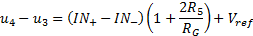
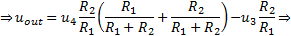
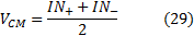
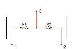
Figure 1. Differential amplifier with gain.
|
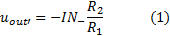
The Differential Amplifier with voltage gain (Figure 1) amplifies the difference between two voltages applied to its inputs as signals. The gain depends on the resistors connected to the OPA and it is also possible to add a reference voltage to the final output. The circuit analysis for the calculation of the output voltage and the gain of the amplifier can be done as follows:
Connect the
IN+
to ground and apply to
IN-
a signal
uin-.
In this way the
A1
is connected as an inverting amplifier and the output voltage is given by the equation:
Then connect the
IN-
to ground and apply to
IN+
a signal
uin+.
In this way the
A1
is connected as a non-inverting amplifier with an input voltage a fraction of the
IN+
because of the voltage divider
R3, R4.
The output is given by:

|
|
The output voltage can be calculated using the superposition theorem with the two cases (1) & (2):

By the equation (3), if
R1=R3
and
R2=R4
and taking into account the
Vref
, is valid:

In the Differential Amplifier with voltage gain the input signals applied through resistor networks to the OPA inputs. This affects the input impedance of the amplifier, which depends on the value of the connected resistors. Moreover, each input seems to have different input impedance than the other. So, if the output impedance of the device applied to the input of the differential amplifier is large or signals with the same or different output impedance are applied
from different devices, both affects the amplifier by decreasing the CMRR.
|
|
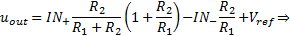
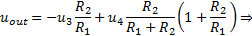
This problem can be solved by using the circuit shown in Figure 2. The circuit is a differential amplifier with voltage gain and it can be found in bibliography as Instrumentation Amplifier with 2 OPA. The first signal (to subtract) is applied to the non-inverting input of
A1,
which is connected as a non-inverting amplifier. The other signal is applied to the non-inverting input of
A2.
The amplified output of
A1
is applied to the inverting input of
A2
and thus the output of
A2
gives the difference between the two signals with a voltage gain and it is also possible to add a reference voltage to the final result. The circuit analysis for the calculation of the output and the voltage gain of the amplifier can be done as follows:
Connect the
IN+
to ground and apply to
IN-
a signal
uin.
Since
IN-=uin
will be also
uA1-=uA1+=uin.
The current through
R1
will be then:

|
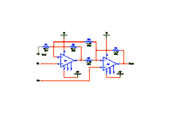
Figure 2. Differential amplifier with 2 OPA.
|
|
Since
IN+=0
will be also
A2-=A2+=0.
The current through
RG
will be then:
The current through
R2
will be then:

The voltage across
R2
will be then:


To the node
RG, R3, R4
is valid:

Since
IN+=0,
as mentioned above, will be also
uA2-=uA2+=0
then the voltage across
R3, R4
will be respectively:

The voltage gain
A
can be calculated from the equations (6), (8), (9), (10) and (11) with the proper replacements:
If
R1=R4
and
R2=R3
finally resulting for gain:
For the circuit analysis the
IN+
is connected to ground and a signal
uin
is applied to
IN-.
This signal is applied to the non-inverting input of
A1.
The output of
A1
however is connected to the inverting input of
A2.
Therefore, the amplified signal applied to the input of
A1
expected to be deducted from the amplified signal applied to
A2.
The equation for the gain (13) is valid to any signal applied to IN+
and finally the output of the amplifier is the difference of the two signals with gain
A:

When applied signals with high frequencies to the Instrumentation Amplifier with 2 OPA there is an asymmetry between the inputs of the signals. The first signal passes through OPA (and especially if it has a large gain) before applied to the differential amplifier for comparison with the other, thus decreasing the CMRR. Also in case an input signal applied to the first amplifier has a
large amplitude or the stage has high gain it is possible to limit its output and thus provide false results.
|
|
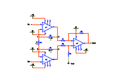
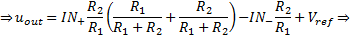
Figure 3. Differential amplifier with 3 OPA.
|
These problems can be overcome by the circuit shown in Figure 3. This circuitis a differential amplifier with voltage gain and it can be found in bibliography as Instrumentation Amplifier with 3 OPA. The signals are applied to the non-inverting inputs of
A1, A2
which are connected as non-inverting amplifiers. The amplified outputs of
A1, A2
are applied to the inputs of
A3
which is connected as a differential amplifier and thus the output of
A3
gives the difference between the two signals with a gain. It is also possible to add to the final result a reference voltage. The circuit analysis for the calculation of the output and the amplifier gain can be made as follows:
The voltage at point 1 equals the
uA-
of
A1
which is equal to signal
IN-
and at point 2 equals the
uA-
of
A2
which is equal to signal
IN+
(due to the differential input of operational amplifiers). Since there is no incoming or outgoing current in the inputs of a OPA, for the current trough
R5, R6, RG
is valid:


|
|
Since the current
i
in the branch
R5, R6, RG
is the same through all resistors and the voltage at points 1 and 2 is known, the voltage at points 3 and 4 can be calculated as follows:

These voltages are the signals applied to the third OPA
A3.
The output can be calculated using the superposition theorem. For the inverting input, connect point 4 to ground and calculate the output based on the voltage at point 3:
For the non-inverting input, connect point 3 to ground and calculate the output based on the voltage at point 4:

By combining the equations (19) and (20) is valid:

And using the superposition theorem is valid:

By the equations (17) and (22), if
R1=R3, R5=R6
and
R2=R4
and taking into account
Vref
, is valid:
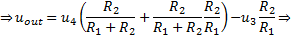


The circuit analysis can be approached alternately as follows: Connect
IN+
to ground and apply to
IN-
a signal
uin-. The point 2 is at ground voltage because of the differential input of OPA.
A1
is connected then as a non-inverting amplifier and its output is given by the equation:

Then connect
IN-
to ground and apply to
IN+
a signal
uin+. The point 2 is at voltage
uin+
because of the differential input of OPA.
A1
is connected then as an inverting amplifier and its output is given by the equation:
And using the superposition theorem is valid:

Repeating the same calculations for
A2:

The signals from the outputs of
A1, A2
are applied to the inputs of
A3
which is connected as differential amplifier with gain. By the equations (26) and (27), and if
R1=R3,
R5=R6
and
R2=R4
and taking into account
Vref
, is valid:
And after some calculations we end up at the same equation as (23):
Common Mode Voltage (CMV) does not amplified in the Instrumentation Amplifier with 3 OPA no matter the gain of amplifier because there is no current flow through
RG
since there is no voltage difference across the resistor due to common signal. Moreover, if common mode differences appear for any reason they tend to eliminate by the output stage witch operates as a differential amplifier.The circuit analysis for the calculation of the CMV can be done as follows: Suppose we apply two signals to the inputs
IN+
and
IN-.
These signals consist of a common mode voltage
VCM
component and a differential voltage
VD
component:
Βy solving the above equations to the terms
IN+
and
IN-:


If the input signals are at the proper level in order to avoid OPA saturation, the current through
RG
is:
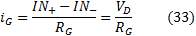
Then the output voltage of
A1
and
A2
are:

|
|
By the equations (33), (34) and (35) is valid:
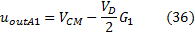
Where:
By the equations (36) and (37) we conclude that only the differential voltage amplified, but not CMV.
A3
is connected as differential amplifier with gain
G3:
From the above equations we conclude that by increasing the gain of the first stage increases CMRR and thus wherein the device needs to operate in gain is useful to maximize the first stage and the second stage operates with a gain of one, if possible. During circuit analysis, in some cases, we accepted that some resistors have exactly the same value. Practically, it is very difficult to match resistors like this. Any discrepancies can cause incorrect results and
reduce the CMRR. Suitable resistances for use in instrumentation amplifiers are resistor networks LT5400 of Linear Technology, where there are four separate resistors in an IC and the matching ratio about 0.01%. Also resistor dividers can be used, like MAX5490, MAX5491, MAX5492 of Maxim or MPM, MPMT of Vishay,
where there are two resistors as a divider in an IC, with the same matching ratio.
|

LT5400 R1=R4, R2=R3
1kΩ,1.25kΩ,10kΩ,100kΩ, 1ΜΩ
Ratio 1:1, 1:4, 1:5, 1:9, 1:10
MPM R1, R2: 250Ω, 500Ω,1kΩ, 2.5kΩ, 5kΩ, 10kΩ, 25kΩ, 50kΩ,
R2: 2kΩ, 4kΩ, 6kΩ, 8kΩ, 9kΩ, 20kΩ, 100kΩ,
Ratio 1:1, 1:2, 1:4, 1:5, 1:6, 1:9, 1:10
|
|
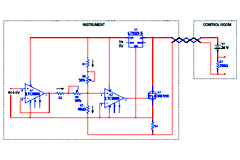
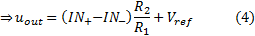
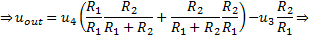
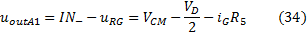
Figure 4. Circuit for measurement instruments 4-20mA.
|
Most of the times, measurement instruments are installed in areas that are far away from the control center where the parameters monitored. It is necessary then, information and power to transferred from one place to the other. The cable’s cost and the possibility of losing information because of electromagnetic noise, especially in industrial areas, are both increasing as distance between instrument and control center
becomes longer. A safe mode for information transferring is by controlling current. This demands only a pair of cables and connects the instrument in the field with the control center. Power for the instrument is also possible to transferred through these cables in order to minimize cost. The most common protocol in industry is 4-20mA where at 4mA corresponds the 0% of the range of the measurement parameter and at 20mA the 100%. This function can be accomplished by the circuit presented at figure 4.
The circuit presented in the right block with the title "CONTROL ROOM" is being installed in the control room where the parameters are monitored. Power supply and equipment for data analysis are being installed in the control room as well. The current, witch regulated by the measurement circuit, develops a potential difference in
R7.
Voltage across
R7
can be converted then to a convenient magnitude by one of the circuits presented above.
The circuit presented in the left block with the title “INSTRUMENT” is being installed in the field where the parameters are measured, together with the sensors and its circuits.
U1
is a voltage stabilizer for power supply to OPAs. The type of
U1
must be low dropout voltage and micropower quiescent current in order be able to stabilize at low input voltage and minimize power consumption below 4mA when idle. Linear Technology LT1521-5 and Microchip MCP1700-5 are suitable ICs for this circuit.
|
|
OPAs must operate normally with the available Voltage supply and within its wide range and also have low power consumption in order to keep the total power consumption below 4mA. Single 5V supply, Rail Input Range – Rail to Rail Output Swing Linear Technology LTC6800 and Microchip MCP617 are suitable OPAs for this circuit.
Q1
may be NPN BJT or N MOS but must have power dissipation above 500mA (
VCE
or
VDS
wil be maximum 24V and
IC
or
ID
maximum 20mA). Suitable devices are BD-139 or IRF-510.
A1
is connected as voltage follower while
A2
is connected as current amplifier.
R1-R5
regulate current
imin
at 4mA when input
IN
is
uIN=0V
, while
R2-R6
regulate
imax
at 20mA when
uIN
is at maximum voltage. The value of
R3
must be greater than value of
R4
(1000 times greater) so current through
R3
be negligible compared with the current through
R4
in order to be valid the approximations for the calculation of
R1, R2
. To calculate
R1
, we consider that
uIN
is 0V and thus output of
A1
is at 0V. 0V is also the potential at the node
R5, R6
due to differential input of
A2
(non-inverting input of
A2
is at GND potential 0V). So there is no potential difference at
R2-R6
and thus the current through
R1-R5
flows through
R3
in which develops a potential difference equal to potential difference at
R4
(R3
and
R4
have a common node at one end and GND at the other). The current through
R4
however is approximately equal to total current consumption of the circuit (current for the operation of the two OPAs and voltage regulator and current through transistor). This current must be
imin
=4mA if
uIN
is 0V. For the following calculation we consider
R1-R5
as one resistor which labeled as
R1
(R5
placed for precision adjustment) and so for
R2-R6
. Is valid then:


R1
can be calculated by solving the equation (40). To calculate
R2
, we consider that
uIN
is maximum (according to the voltage regulator LT1521-5) and thus
uIN
is the potential at output of
A1
. There is a potential difference at
R2
then and the current through
R3
is the sum of the currents through
R1
and
R2
. Moreover, the current through
R4
must be
imax
=20mA if
uIN
is at maximum value. Is valid then:


R2
can be calculated by solving the equation (41) (R1
is already known).
|
| |
|
|
|
Thank you for your support to make my website better.
|
© 2017 Dimitrios Porlidas
|
|
|


