|
 
|
|
Electronic cash register with fiscal memory
The following project describes the method of implementation of an Electronic Cash Register with Fiscal Memory. The device contains the modules to perform all necessary operations (add, multiply, calculate taxes, print receipts and store information in an EEPROM). The system architecture is based on the
transmission of data between microcontrollers, which control subsystems, via I2C bus. Subsystems that structure layout are the display unit, the printing unit, the central processing unit and the fiscal memory. The microcontrollers used are AVR ATmega8 and ATmega32 and the printer is Citizen DP630.
|
|
Author: Dimitrios Porlidas
Curriculum Vitae
 electronics@porlidas.gr electronics@porlidas.gr
 Facebook Facebook
 Linkedin Linkedin
|
|

|
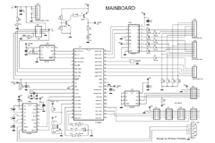
The Electronic
Cash Register (ECR) consists of seven different modules:
Main Board (MB), Printer (Prt), Printer Board (PB), Display Board (DB),Keyboard, In System Programmer (ISP) and Power Supply (PS).
The MB
module is host to Microcontroller Unit (MCU) that executes all the process. It has
back up voltage from rechargeable battery (NiMH 650mAh) for the needs of MCU and Real Time Clock (RTC). It also incorporates I2C bus and Keyboard interface.
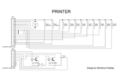
The Printer is dot matrix and prints in two paper strips of 37mm. The PB attends the
printing interface; communicates with MCU via I2C. The system architecture
allows changing printing method or type of printer only by changing PB and Printer.
|
|
The DB displays the charges and the calculations; communicates with MCU via I2C. The system architecture again allows changing displaying method or type of display only by changing DB.
The Keyboard is connected directly to MCU and consists only by switches. ISP exists for programming MCU in order to upgrade software or extend features in ECR. The PS module provides 5V DC for all digital and analog circuits and 24V DC for Printer's motor and print head.
As
mentioned above, the MB module is host to a MCU, which is ATmega32, a RTC, which is
DS1302 and also incorporates I2C bus and Keyboard interface. DS1302
communicates with MCU at $09 via a simple serial interface connected to port PB0-2.
It communicates only when issuing print reports, writing data to fiscal memory
or adjusting its time and date. In all other cases is in Timekeeping mode (Osc
On) and the power consumption is 1μA.
|

|
|
|
I2C bus is
connected directly to MB's MCU because it has the hardware to support it. MCU is the master of the bus at $01. There are 4 sockets for connecting devices. The three of them are identical, having SDA and SCL signals and 5V power lines (V1 and
GND) and used to connect the Printer and Display units while third socket is spear. The
fourth is for the connection of fiscal memory and contains Write Protect (WP)
signal more. In MB there
is also a socket for ISP in order to upgrade MCU’s software, and a RS232 USART port
with the necessary components (MAX232 and capacitors) for future usage.
The power
supply for the MCU (and the RTC) is from VccAcc. When operating the power
supply (V1=5V) T1 is in saturation because of voltage divider R2-R3 and so T2
is in saturation because of T1 thus VccAcc~5V (while charging the battery
through R1). When not operating
the power supply (V1=0V) T1 is in cutoff. The battery then reverse biases the
contact CE of T2 thus not conducting, isolating the VccAcc from the power
supply circuit. VccAcc at this time is equal to battery voltage.
|
|
The MCU is
in normal operation when the voltage V1=5V and goes into Sleep mode when V1<4.7V.
When V1=5V T3 is in saturation because of voltage divider R17-R18 thus PD2 is
in logic 0 (normal operation). When V1 begins to fall, and becomes less than
4.7V, T1 goes to cutoff thus PD2 goes to logic 1 because of R5 and VccAcc. The
MCU then performs a routine during which stores the contents of the registers
in RAM, programming all ports as outputs to logic 0 except PD2 which
programming as IRQ INT0, and goes into Sleep mode. The total power consumption
at this state is 23μA according
to measurements. Logic 0 in
INT0 (because of restoring of V1) brings back MCU to normal operation recovering
data and previous state.
Keyboard interface occupies port A while 74HC238 is used to extend the interface for more
buttons. The MCU, during start up, programs
PA0-3 ports as outputs and PA4-7 ports as inputs with internal Pull up resistors disabled. In inputs placed external Pull down resistors which provide logic 0 when not pressed any button or in case of disconnection of the
keyboard.
|

|
|

|
The outputs PA0-2 are connected to the inputs of the 74HC238, while PA3 is connected to a buzzer
for key press sound indication. The outputs of the 74HC238 Y0-6 are connected
in columns of a keyboard matrix 4x7 through diodes, while Y7 is connected to common
of a four positions contact selector, which determines the cash register’s mode
(OPER, X, Z, PROG). The lines of the keyboard and the four positions of the
selector switch are connected to the inputs of the microcontroller PA4-7.
During program execution, the MCU increases PA0-2 from $00 to $07 and monitors the content of PINA.
If is greater than $07, the program is checking the position of the selector.
If PINA does not match to none of the positions of the selector it means that a
button is pressed and waiting to be released. When the button released, the
program checks the condition that verifies the contents of the register,
activates the buzzer and performs the appropriate operation.
|
|
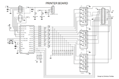
The PB
consists of a MCU, which is ATmega8, and 3 integrated circuits for the power amplifiers for
the printer. It communicates with the MB’s MCU via the I2C bus at $06 (as a
slave). PD0-7 and PC0-2 ports are programed as outputs while PB0-2 ports are
programed as inputs. PD0-7 ports are connected to the power amplifier driving
the pins of the printer head while PC0-2 ports are connected to the power
amplifier driving the motor and the coils for the paper strip forwarding. PB0-2
ports receive signals from the printer, which indicate the position of the
head.
The amplifying stage consists of three STA401A. Each one has integrated 4 pairs Darlington
transistors, diodes and bias resistors. Each Darlington can provide 3A current. D1-11
diodes are used to avoid applying high voltage to PB's MCU in case of failure of STA401A
and short circuit. The diodes are in reversed bias then whatever is the status of
the outputs of MCU.
|
|
|

|
The printer has a DC motor which drives a gear system to move the print head and to forward
the paper strip and ribbon. Two discs with notches are mounted to the motor
shaft and together with a led and a phototransistor trace the movement of
the print head and so MCU controls typing routine. A switch at the one end of the print head's route determines
its position.
During program
execution, the PB's MCU is watching I2C bus for data received and starts printing
sequence in case of receive a package. Every package consists of ASCII
characters. The PB's MCU uses a matrix stored in to convert ASCII characters to columns of dots and print them. Each character consists of 5 columns and there are two blank columns between characters. For each column energized the pins of the print
head for 0.5ms. Each line can have 15 characters. At the end of each line in order to forward
the paper strip energized the coils for 7.5ms.
|
|
|
|
|
|
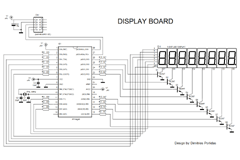
The DB
consists of a MCU, which is ATmega8, eight Seven Segment Display LED type and
transistors for multiplexing the displays. It communicates with the MB’s MCU via
the I2C bus at $05 (as a slave).
All
Segments of Displays are connected in parallel to the ports PD0-7 of the DB’s
MCU which are programed as outputs. Resistors R1-8 limit the current to the LEDs
of Displays so that, even if all LEDs light up, not to overload MCU. The common
cathodes of Displays are connected to transistors Q1-Q8. Each Display energized
by its transistor for 2.5ms. The bases of the transistors are connected tothe ports PC0-3 and PB1-4 through
resistors R9-16, which are programed as outputs too.
|

|
|
|
During program execution, the DB's MCU is watching I2C bus for data received. Data are numbers in ASCII
characters and when received, the MCU uses a matrix stored in to convert them
and display the numbers to Seven Segment Displays. The numbers displayed in
reverse order, so that each new number entered from the keyboard to occupy the
first position to the right and the others to shift one position left. The DB's MCU
executes the appropriate routines for multiplexing as well. The MB’s
MCU keeps in a register the content of displays and each time recovers from
Sleep Mode send it to DB because the power supply of DB is V1 through I2C socket and DB’s MCU
turns off when V1 falls.
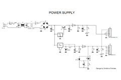
The power supply unit operates with mains electricity (230V AC) and
produces stabilized voltages 5V DC and 23.3V DC. It consists of a toroidal transformer 24V AC
100VA, a rectifying stage, a stabilized step down switching power supply 5V/3A
DC and a stabilized linear power supply 23.3V DC. The power supply is more powerful
than the requirements of the system.
|
|
A safety
circuit mounted to 5V power line in order to avoid applying high voltage to
electronic circuits in case of 5V power supply failure. It consists of a 6.2V
Zenner diode (D3) and a Thyristor (T1). If the
voltage in 5V power line exceeds 6.2V (Zenner voltage) the thyristor goes over conductivity state and so burned the fuse (F4) isolating the 5V power line.
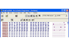
Fiscal memory is normally not part of the motherboard, but it's a different system in a
remote location. It communicates with the rest of the device through a bus and
is used as storage medium for tax information. For simplicity integrated on the
motherboard, but without having any electrical connection with the rest of the board
but only through a ribbon cable only so it is possible to cut the piece that is
developed and remove it. The entries are in hexadecimal system, except date
that is written on BCD. Each record occupies 32 bytes and consists of 11
fields: 1 starting byte (AA), 1 byte featuring reliable recording (FF), 3 bytes
for date, 2 bytes for the serial number of the record, 6 fields of 4 bytes each
for tax information and 1 byte for validation using CRC. Below there is an
example of two records as read by the I2C EEPROM Reader - Programmer.
|

|
|
|

|
|
| |
|
|
|
Thank you for your support to make my website better.
|
© 2017 Dimitrios Porlidas
|
|
|


